
HiFi Streaming
#9 in a series of articles about wander and jitter
In order to talk about WHEN we care about jitter, we have to separate jitter into the categories of Data Jitter and Sampling Jitter
In the case of Data Jitter, our only real worry is that the data transmission doesn’t get bit errors. In almost all cases, this should be taken care of by the equipment itself – or the components inside it. If you have a device with a digital output, hopefully, that output has been tested to ensure that it meets the standards set for it. If it’s an AES/EBU output, then it meets those standards. If it’s an S-PDIF coaxial output, then it meets those standards. This doesn’t just mean that the data coming out of that output is correct. It also means that the output impedance of the hardware is correct, the voltage levels are correct, and so on. They have to meet the standard requirements. This is easily testable if you have the correct equipment. I won’t mention any brands here because there are many.
The same is true for a digital input. Either it meets the appropriate standard, and it works, or it doesn’t – and this will be the fault of the manufacturer and the supplier of the components inside. However, again, the input must have the correct input impedance, be able to accept the correct voltage ranges, and meet the specifications for the transmission protocol with respect to jitter immunity. This is one of the nice things about digital audio transmission protocols like AES/EBU and S-PDIF. The standards assume that there will be some jitter in the transmission system, and the receiver must be able to withstand this (remember we’re specifically talking about data jitter here). This is tested by intentionally adding jitter to a signal sent to the device, and looking at the errors at its output. The standards state thresholds for jitter – meaning that if you do induce (or accidentally have) jitter under that threshold, you must get no errors. If you do, then you don’t meet the standards.
The only thing left then, is the cable that connects the input and the output devices. In order to ensure that the system behaves as intended, you are best to use a cable with the correct impedance. I will not get into what this means. If you are using AES/EBU over an XLR cable, then it should be a cable with a 110 Ω impedance. If you are sending S-PDIF over a coaxial cable, then it should be a 75Ω cable. If you do not use cables with the correct impedance, you will get some amount of reflection on the connection. However, the amount that you need to worry about this is proportional to the length of the connector. In other words, the longer the cable, the more you should worry about it.
Sampling jitter will only happen:
The real question in the second and third of these cases is how good the device itself (the DAC or the ASRC) is at attenuating jitter. We can assume that jitter exists on the connections between devices – and inside devices. The real question is how well the device or components reduce the problem. For example, if you have a DAC that uses the incoming digital signal as the clock, and that external clock has jitter for some reason (we can assume that it does) , can the DAC reduce the timing errors? If it’s implemented well, then the answer is “yes”. It can smooth out the timing errors in the incoming sampling rate (using a PLL and/or an ASRC, for example) and create a new, clean clock.
In other words, if your source has jitter, but is within the standard for the transmission protocol, and your DAC is designed to attenuate jitter adequately, then the amount of jitter in the source is irrelevant (within reason).
However, if your DAC tracks the incoming sampling rate and uses it as the clock, and the source has jitter (but is within the standard) then the amount of jitter at the source’s output is not irrelevant.
So, unfortunately, there’s no simple answer that can tell you when you need to worry about jitter. It really depends on the specific abilities of your various devices and the components inside them.
Footnote: There is one notable exception to my statement that the ADC’s are the recording studio’s problem and not yours. This exception occurs when you have an analogue signal coming into a digital audio device. For example, if you have a turntable or a cassette deck going through a preamp or AVR with DSP. Another example is a loudspeaker with an analogue input, but DSP-based processing.
The simple answer to this these days is “probably not”.
The reason I say this is that, in modern equipment, jitter is very unlikely to be the weakest link in the chain. Heading this list of likely suspects (roughly in the order that I worry about them) are things like
So, if none of these cause you any concern whatsoever, then you can start worrying about jitter.
#8 in a series of articles about wander and jitter
Although I am guessing, I don’t think that it is crazy to say that the majority of digital audio systems today employ some kind of sampling rate conversion somewhere in the signal flow.
A sampling rate converter is a physical device or a processing block in some software that takes an audio signal that has been sampled at one rate (say, 44.1 kHz) and converts it to an audio signal at another rate (say, 48 kHz).
There are many reasons why you might want to do this. For example, if you have a device that has equalisation (filtering), then if you change the sampling rate, you will have to new coefficients into the filters. If you have a LOT of filters, then it might take so much time to load them into the system that you’ll miss the first second or two of a song if it’s a different sampling rate than the previous song. So, instead of doing this, you keep your processing at one constant (or ‘fixed’) sampling rate, and convert the input to that rate. This might even be true in the case where the incoming sampling rate is the same as the internal sampling rate. For example, you might be “sample rate converting” from 48 kHz to 48 kHz – just to keep the design of the system clocking constant.
Looking very broadly, there are two options for sampling rate conversion.
Synchronous Sampling Rate Conversion
Let’s say that you have to convert from 48 kHz to 96 kHz – a multiplication of 2. In this simple case, you could take the incoming samples, and insert an new, extra one mid-way between each of them. The value of the new sample depends on how you are doing the math to calculate it. We will not discuss this here. The important thing about this concept is that the timing of the output is “locked” to the input. In this example, every second sample of the output happens at exactly the same time as every sample at the input. This can also be true if the ratio of the sampling rates are not “nicely” related like a 2:1 ratio. For example, if you have an input at 44.1 kHz and and output at 48 kHz, you could take the incoming 44.1 kHz signal, insert 47999 “virtual” samples between each of the original samples (making the new sampling rate 2116800000 Hz) and then pull an output sample from that stream every 444100 samples.
In other words:
(44100 * 48000) / 44100 = 48000
Of course, this is not a smart way to do this (because it will be a huge waste of processing power and memory – and imagine how big the numbers would be if you’re converting 176.4 kHz to 192 kHz… bigger!), but it would work, as long as the “virtual” samples you create at the very high “virtual” sampling rate have the correct values.
This type of sampling rate conversion, where the output is numerically “locked” to the input in time (meaning that, at some regular interval of time, the input and the output samples will happen simultaneously – or at least with a constant delay) is called synchronous sampling rate conversion. It’s called that because the input and the output are synchronised with each other… A bit like gears meshing together.
Asynchronous Sampling Rate Conversion
There is another way to do this, where we do not lock the output clock to the input clock. Let’s say that you want to build a device that has a constant sampling rate at its output, but you don’t really know what the sampling rate of the input is. In this case you will use an asynchronous sampling rate converter – so-called because there is no fixed lock between the input and output clocks.
In this case, the incoming signal is analysed and its sampling rate is measured. The way this is done is a little similar to the method shown above. You take the clock running at the rate of the output’s signal and multiply that by some value (say 512, for example) to create an internal “virtual” clock running at a higher sampling rate. You then “grab” the value of an incoming sample and apply its value to the “virtual” sample that is closest in time. This allows the incoming samples to drift in time relative to the output samples.
In both cases, there is the open question of how you generate the signal at the higher internal sampling rate. This can be done using a kind of low pass filter that is effectively similar to the reconstruction filter in a DAC. I will not talk about this any more than that – other than to say that the response characteristics of that filter are VERY important… So, if you’re planning on building your own sampling rate converter, read a lot more stuff on the subject than what I’ve written here – because what I’ve written here is most certainly not enough information.
There’s one strange effect that pops up here. Since, in an ASRC (Asynchronous Sampling Rate Converter) the incoming signal is sampled at discrete times that are numerically related to the output sampling rate, then any potential jitter in the system is also quantised in time. So, for example, if your output sampling rate is 48000 samples per second, and you’re creating the internal sampling rate by multiplying that by 512, then any jitter in the ASRC cannot have a value less than 1/(48000*512) second = 4.069*10^-8 or 40.69 nanoseconds. In other words, in such a system, the error caused by jitter will be 0, ±40.69 nanoseconds, ±81.38 nanoseconds, and so on. It can’t be something in between… (assuming that the output clock is perfect. If it’s drifting due to jitter, then those values will also drift…)
The good news is that, if the clock that is used for ASRC’s output sampling rate is very accurate and stable, and if the filtering that is applied to the incoming signal is well-done, then an ASRC can behave very, very well – and there are lots of examples of this. (Sadly, there are many more examples where an ASRC is implemented poorly. This is why many people think that sampling rate converters are bad – because most sampling rate converters are bad.) in fact, a correctly-made sampling rate converter can be used to reduce jitter in a system (so you would even want to use it in cases where the incoming sampling rate and outgoing sampling rates are the same). This is why some DAC’s include an ASRC at the input – to reduce jitter originating at the signal source.
Wrapping up Part 8: The take-home messages for these three parts in Section 8 are:
Addendum. If you want to dig further into the world of Sampling Jitter and the advantages of using ASRC’s to attenuate jitter, I highly recommend the following as a good starting point:
#8 in a series of articles about wander and jitter
In the previous post we looked at the effect of an incoming analogue signal that is sampled at the wrong times. In that description, I implied that the playback of the samples would happen at exactly the correct times. So, the jitter was entirely at the ADC (analogue-to-digital converter) and nowhere else.
In this posting, we’ll look at a very similar issue – jitter in the DAC (digital-to-analogue converter).
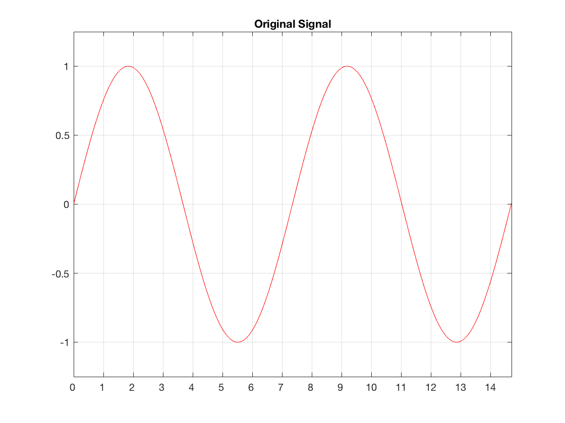
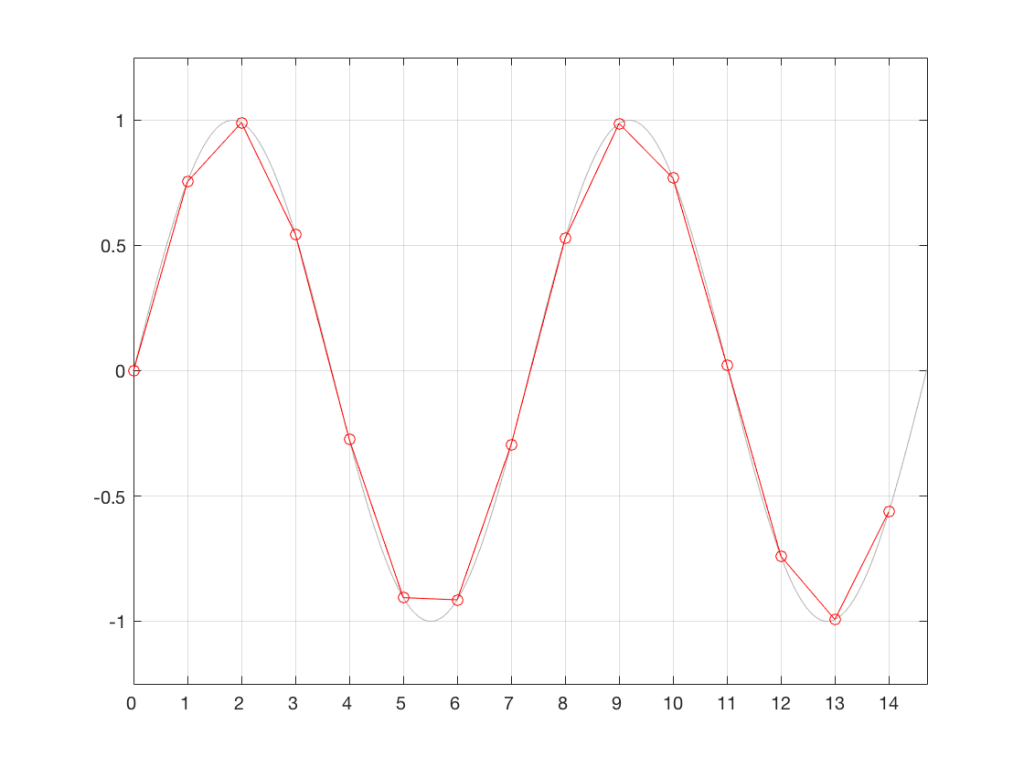
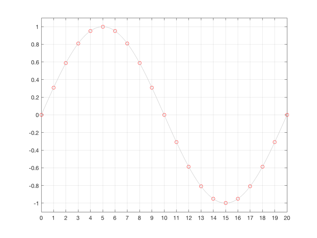
Let’s assume that we have a signal (in our case, a sinusoidal waveform, since that’s easy to plot) that was sampled by an ADC with no jitter. So, our original signal looks like Figure 1.
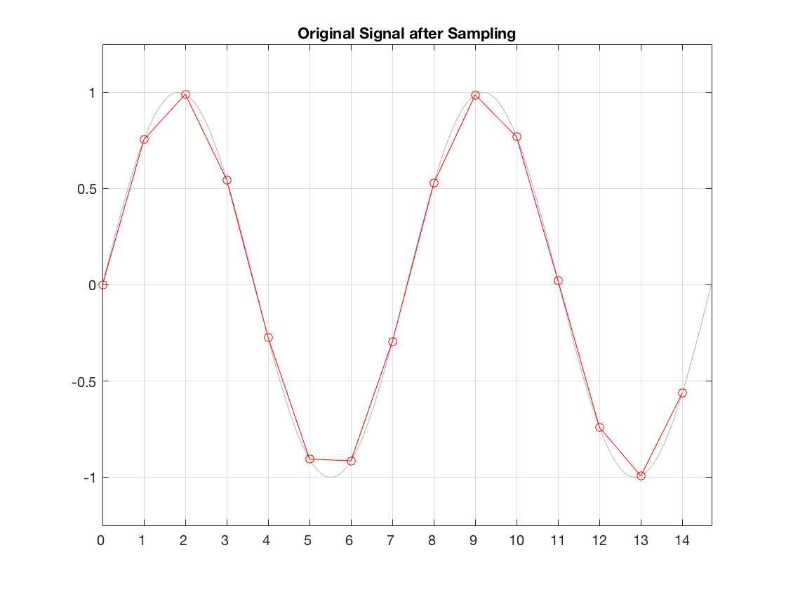
That signal is sampled by the ADC at exactly the correct times, since it has no jitter. The result of this is shown below in Figure 2.
When the time comes to play this signal, we send those samples to the DAC in the correct order and hope that it converts each of them to an analogue voltage at exactly the correct times. If the sampling rate of the system is 96 kHz, then we hope that the DAC converts a sample ever 1/96000th of a second, at exactly the right time each time.
That time that the DAC spits out the sample is dictated by a clock somewhere in the system. It might by an internal clock, or it might come from an external device, depending on your system and how it’s being used. However, if that clock is inaccurate for some reason, or if there is some kind of noise infecting the connection between the clock and the DAC, then the DAC can be triggered to convert a sample at the incorrect time. This is sampling jitter in the digital to analogue conversion process. I’ve tried to illustrate this in Figure 3.
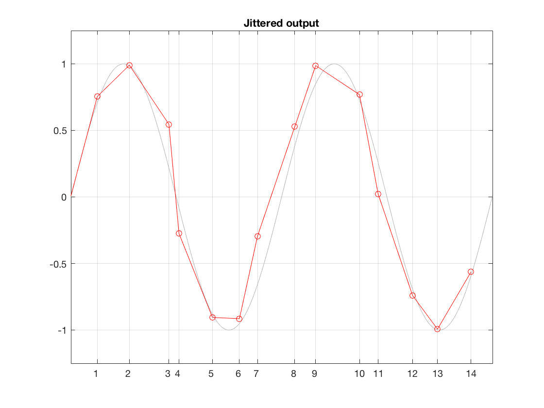
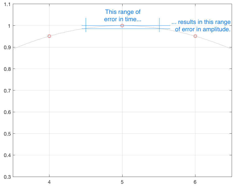
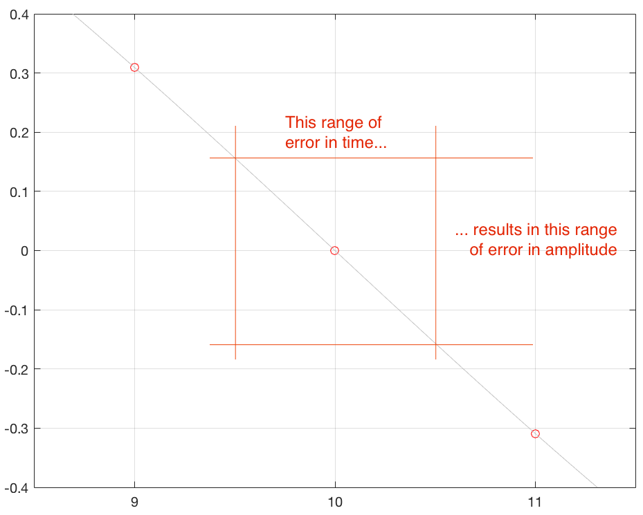
It may not be immediately obvious, but the sample values in Figure 3 are identical to those in Figure 2. What I’ve done is to move them in time, so that you’re getting exactly the right level output at the wrong time each time. Of course, I have heavily exaggerated this plot to make it obvious that the times between consecutive samples are not equal. Some are much shorter than the sampling period (e.g. between samples 3 and 4) and some are much longer (e.g between samples 9 and 10).
Just like the case of ADC jitter, we can analyse this simply as an amplitude error. In other words, as a result of the timing errors, the red circles are not sitting directly on the original gray signal. And, just like we saw in the case of the ADC jitter, the amount of amplitude error is proportional to the slope of the signal.
Addendum: It’s important to remember that the descriptions and the plots that I’m showing here are to help show what jitter is – and those plots are high. I’m not showing what the final result will be. The actual jitter in a system is much, much lower than anything I’ve shown here. Also, I’ve completely omitted the effects of the anti-aliasing filter and the reconstruction filter – just to keep things simple.
#8 in a series of articles about wander and jitter
Ignoring a most of the details, converting an analogue audio signal into a digital one is much like filming a movie. The signal (a continuous change in voltage) is measured (or sampled) at a regular rate (the sampling rate), and those measurements are stored for future use. This is called Analogue-to-Digital Conversion.
In the future, you take those samples, and you convert them back to voltages at the same sampling rate (in the same way that you play a film at the same frame rate that you used to record it). This is called Digital-to-Analogue Conversion.
However, we’re not here to talk about conversion – we’re here to talk about jitter in the conversion process.
As we’ve already seen, jitter (and wander) is an error in the timing of a clock event. So, let’s look at this effect as part of the sampling process. To start: jitter in the analogue to digital conversion.
Let’s say that we want to convert an analogue sinusoidal wave into a PCM digital version.
Note that I’m going to skip a bunch of steps in the following explanation – concentrating only on the parts that are important for our discussion of jitter.
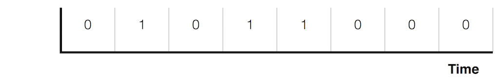
We start with a wave that has theoretically infinite resolution in amplitude and time, and we divide time into discrete moments, represented by the numbered vertical lines in the plot below.
Every time the clock “ticks” (in other words, on each of those vertical lines), we measure the voltage of the signal. These discrete measurements are represented in Figure 2 as the circles, sitting on the original waveform (in gray).
Part of this system relies on the accuracy of the clock that’s used to tell the sampling system when to do the measurements. In a perfect world, a system with a sampling rate of 44.1 kHz would make a measurement of the incoming analogue wave exactly every 1/44100th of a second. The time between samples would never vary.
This, of course, is impossible. The clock that ticks at the sampling rate will have some error in time – albeit a very, very small error.
Let’s heavily exaggerate this error so that we can see the resulting effect. Figure 3 shows the same original analogue sinusoidal waveform, sampled (measured) at incorrect times. In other words, sometimes the measurement (represented by the red circles) is made slightly too early (to the left of the gray vertical line – as is the case for Sample #9), sometimes, it’s made too late (to the right of the line – as in Sample #2).
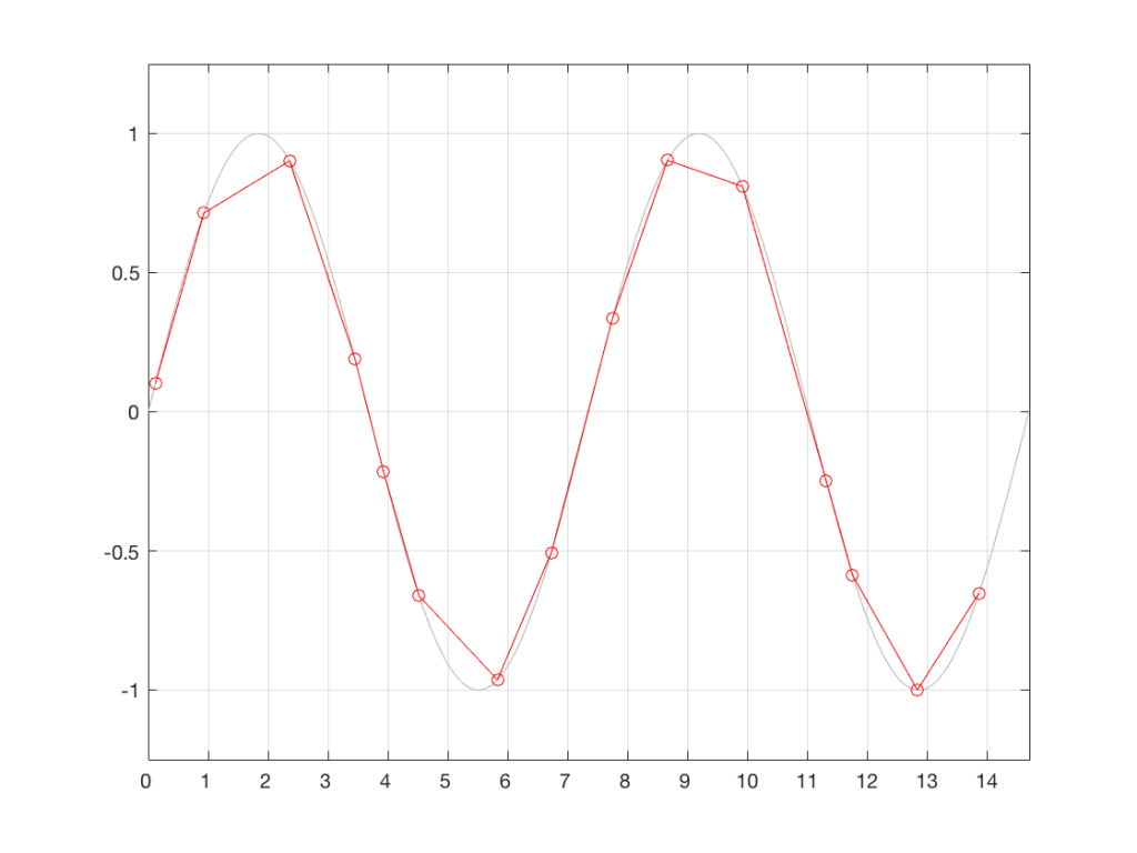
For example, look at the sample that should occur at clock tick #2. I’ve zoomed in to the plot so that this can be seen more clearly in Figure 4.
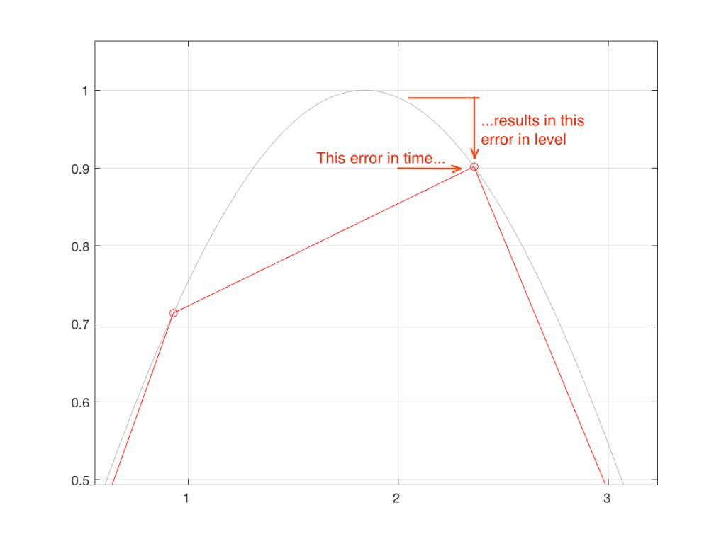
Notice that, because the measurement was made at the wrong time (in the case of sample #2, somewhat late), the result is an error in the measurement of the waveform’s amplitude. So, an error in time produces an error in level.
Let’s assume that the measurements we made in Figure 3 are stored and then replayed at exactly the correct times – what will the result be? This is shown in Figure 5. As you can see there, by comparing the measurements we made in Figure 3 to the original waveform, we have resulted in a distortion of the waveform.
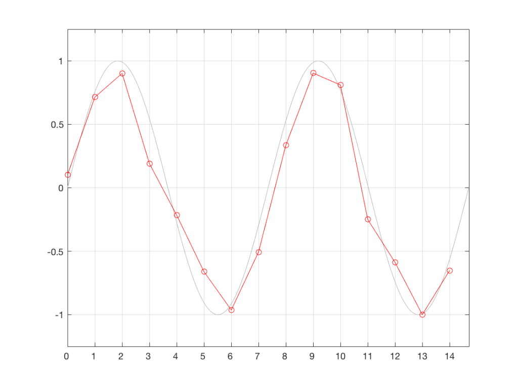
The time-based errors in the measurements in Figure 3 result (in this example) in a system that contains amplitude-based errors at the output. This results in some kind of distortion of the signal, as can be seen here.
As you can see in Figure 5, the result is a signal that is not a sine wave. Even after this digital signal has been low-pass filtered by the reconstruction filter in the Digital-to-Analogue Converter (the DAC), it will not be a clean sine wave. But let’s think about exactly what can go wrong here, more carefully.
For starters, an error that is ONLY caused by timing errors in the sampling process cannot produce levels that are outside the amplitude range of the original signal. In other words, if our original signal was 1 V Peak and symmetrical, then the sampled waveform will not exceed this. This is because the samples are all real measurements of the signal – merely performed at the incorrect times.
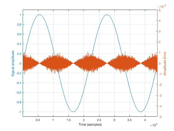
Secondly, if the amount of jitter is kept constant, then the amount of amplitude error will modulate (or vary) with the slope of the signal. This is illustrated in Figure 6, below.
Another way to consider this is that, given a constant amount of jitter, the amplitude error (and therefore the distortion that is generated) modulates with the signal, is proportional to the slope of the signal. Since the maximum slope of the signal increases with amplitude and with frequency, then jitter artefacts will also increase as a result of an increase in the signal level or its frequency.
Thirdly, (and this one may be obvious): in an LPCM system, there are no jitter artefacts if there is no signal. If the input signal is constantly 0, then it doesn’t matter when you measure it… (Note that I said “in an LPCM system” in that sentence – if it’s a Delta-Sigma (1-bit) converter, then this is not true.)
There is more thing to consider – although, given the level of jitter in real-life systems these days, this one is more of a thought experiment than anything else. Take a look back at Figure 3 – specifically, the samples that should have been taken at times 11 and 12. In a 44.1 kHz system, those two samples would have been samples 1/44100th of a second apart. However, as you can see there, the time between those two samples is less than 1/44100th of a second. If the sampling period is reduced, then the sampling rate must be higher than 44.1 kHz. This means that, ignoring everything else, the Nyquist frequency of the system is momentarily raised, allowing content above the intended Nyquist into the captured signal… However, as I said, this is merely an interesting thing to think about. Find something else to feed your free-floating anxiety that keeps you up at night – this issue is not worth a wink’s worth of lost sleep…
One extra thing to note here: If you look at Figure 3, you see a signal that has artefacts caused by jitter. Simply stated, this means that there are errors in the recorded signal. The way I’ve plotted this in Figure 3, those can be considered to be amplitude errors when played through a system without jitter. In other words, if you have a signal with jitter artefacts, you cannot remove them by using a system that has no jitter. the best you can do is to not add more jitter…
Addendum: This description of jitter artefacts as an amplitude distortion is only one way to look at the problem – using what is called the “Time-Domain Model”. Instead, you could use the “Frequency-Domain Model”, which I will not discuss here. If you’d like to dive into this further, Julian Dunn’s paper called “Jitter Theory” – Technical Note TN-23 from Audio Precision is the best place to start. This is a chapter in his book called “Measurement Techniques for Digital Audio”, published by Audio Precision. See this link for more info.
#7 in a series of articles about wander and jitter
Back in a previous posting, we looked at this plot:
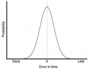
The plot in Figure 1 shows the probability of a timing error when you have random jitter. The highest probability is that the clock event will happen at the correct time, with no error. As the error increases (either earlier or later) the probability of that happening decreases – with a Gaussian distribution.
As we already saw, this means that (if the system had an infinite bandwidth, but random jitter) the incoming signal would look something like the bottom plot in Figure 2 when it should look like the top plot in the same Figure.
However, Figure 1 doesn’t really give us enough information. It tells us something about the timing error of a single event – but we need to know more.
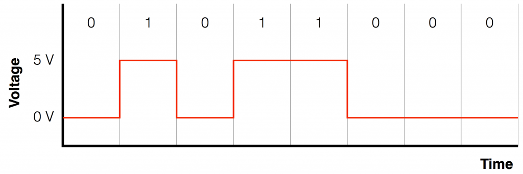
Sidebar: Encoding, Transmitting, and Decoding a bi-phase mark
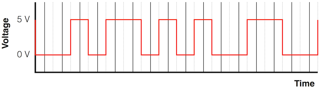
Let’s say that you wanted to transmit the sequence of bits 01011000 through a system that used the bi-phase mark protocol (like S-PDIF, for example). Let’s walk through this, step by step, using the following 7 diagrams.
At this point, the receiver has two pieces of information:
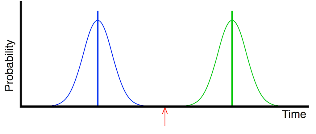
The probability plot in Figure 1 shows the distribution of timing errors for a single clock event. What it does not show is how that relates to the consecutive events. Let’s look at that.
Let’s say that you have two consecutive clock events, represented in Figure 10, below, as the vertical Blue and Green lines. If you have jitter, then there is some probability that those events will be either early or late. If the jitter is random jitter, then the distribution of those probabilities are Gaussian and might look something like the pretty “bell curves” in Figure 10.
Basically, this means that the clock event that should happen at the time of the vertical blue line might happen anywhere in time that is covered by the blue bell curve. This is similarly true for the clock event marked with the green lines.
If we were to represent this as the actual pulse wave, it would look something like Figure 11, below.
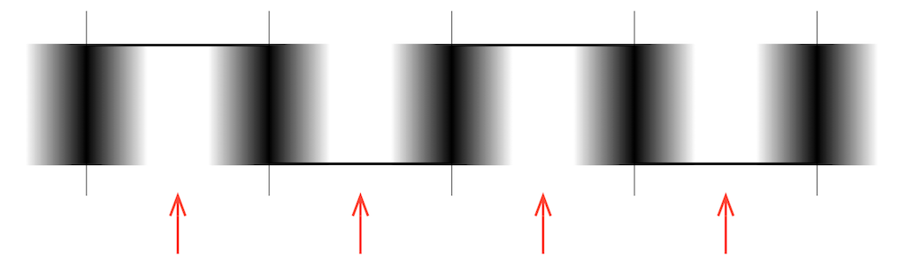
You will see some red arrows in both Figure 10 and Figure 11. These indicate the time between detected clock events, which the receiver decides is the “safe” time to detect whether the voltage of the carrier signal is “high” or “low”. As you can probably see in both of these plots, the signal at the moments indicated by the red arrows is obviously high or low – you won’t make a mistake if you look at the carrier signal at those times.
However, what if the noise level is higher, and therefore the jitter is worse?
In this case, the actual clock events don’t move in time – but their probability curves widen – meaning that the error can be earlier or later than it was before. This is shown in Figure 12, below.
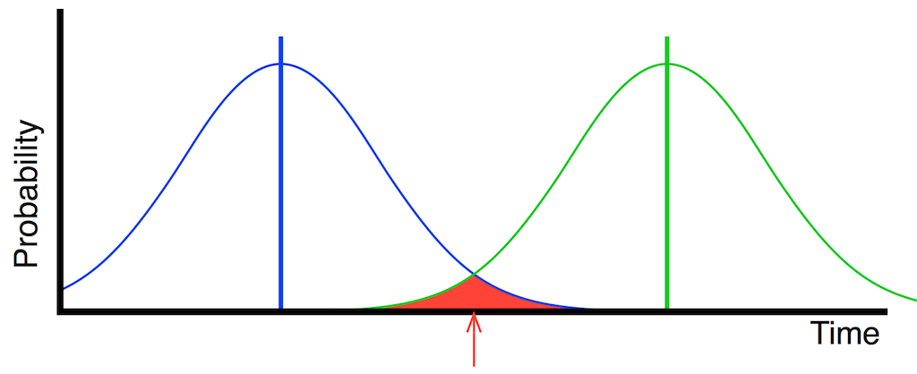
If you look directly above the red arrow in Figure 12, you will see that both the blue line and the green line are there… This means that there is some probability that the first clock event (the blue one) could come AFTER the second (the green one). That time reversal could happen any time in the range covered by the red area in the plot.
An artist’s representation of this in time is shown in Figure 13, below. Notice that there is no “safe” place to detect whether the carrier signal’s voltage is high or low.
If this happens, then the sequence that should be interpreted as 1-0 becomes 0-1 or vice versa. Remember that this is happening at the carrier signal’s cell rate – not the audio bit rate (which is one-half of the cell rate because there are two cells per bit) – so this will result in an error – but let’s take a look at what kind of error…
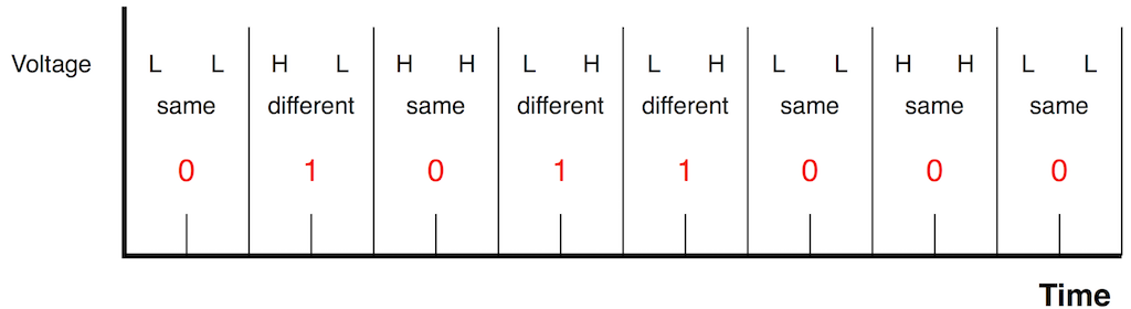
The table below shows a sequence of 3 binary values on the left. The next column shows the sequence of High and Low values that would represent that sequence, with two values in red – which we assume are reversed. The third column shows the resulting sequence. The right-most column shows the resulting binary sequence that would be decoded, including the error. If the binary sequence is different from the original, I display the result in red.
You will notice that some errors in the encoded signal do not result in an error in the decoded sequence. (HH and LL are reversed to be HH and LL.)
You will also notice that I’ve marked some results as “Invalid”. This happens in a case where the cells from two adjacent bits are the same. In this case, the decoder will recognise that an error has occurred.
[table]
Original, Encoded, Including error, Decoded
000, HH LL HH, HH LL HH, 000
,HH LL HH, HL HL HH, 110
, HH LL HH, HH LL HH, 000
,HH LL HH, HH LH LH, 011
, HH LL HH, HH LL HH, 000
001, HH LL HL, HH LL HL, 001
, HH LL HL, HL HL HL, 111
, HH LL HL, HH LL HL, 001
, HH LL HL, HH LH LL, 010
, HH LL HL, HH LL LH, Invalid
010, HH LH LL, HH LH LL, 010
, HH LH LL, HL HH LL, 100
, HH LH LL, HH HL LL, Invalid
, HH LH LL, HH LL HH, 000
, HH LH LL, HH LH LL, 010
100, HL HH LL, LH HH LL, Invalid
, HL HH LL, HH LH LL, 010
, HL HH LL, HL HH LL, 100
, HL HH LL, HL HL HL, 111
, HL HH LL, HL HH LL, 100
011, HH LH LH, HH LH LH, 011
, HH LH LH, HL HH LH, 101
, HH LH LH, HH HL LH, Invalid
, HH LH LH, HH LL HH, 000
, HH LH LH, HH LH HL, Invalid
110, HL HL HH, LH HL HH, Invalid
, HL HL HH, HH LL HH, 000
, HL HL HH, HL LH HH, Invalid
, HL HL HH, HL HH LH, 101
, HL HL HH, HL HL HH, 110
111, HL HL HL, LH HL HL, Invalid
, HL HL HL, HH LL HL, 001
, HL HL HL, HL LH HL, Invalid
, HL HL HL, HL HH LL, 100
, HL HL HL, HL HL LH, Invalid
[/table]
As you can see in the table above, for the 5 possible errors in the encoded stream, the binary sequence can have either 2, 3, or 4 errors (or invalid cases), depending on the sequence of the original signal.
If we take a carrier wave that has random jitter, then its distribution is Gaussian. If it’s truly Gaussian, then the worst-case peak-to-peak error that’s possible is infinity. Of course, if you measure the peak-to-peak error of the times of clock events in a carrier wave (a range of time), it will not be infinity – it will be a finite value.
We can also measure the RMS error of the times of clock events in a carrier wave, which will be a smaller range of time than the peak-to-peak value.
We can then calculate the ratio of the peak-to-peak value to the RMS value. (This is similar to calculating the crest factor – but we use the peak-to-peak value instead of the peak value.) This will give you and indication of the width of the “bell curve”. The closer the peak-to-peak value is to the RMS value (the lower the ratio) the wider the curve and the more likely it is that we will get bit errors.
The value of the peak-to-peak error divided by the RMS error can be used to calculate the probability of getting a data error, as follows:
[table]
Peak-to-Peak error / RMS error, Bit Error Rate
12.7, 1 x 10⁻⁹
13.4, 1 x 10⁻¹⁰
14.1, 1 x 10-11
14.7, 1 x 10-12
15.3, 1 x 10-13
[/table]
The Bit Error Rate is a prediction of how many errors per bit we’ll get in the carrier signal. (It is important to remember that this table shows a probability – not a guarantee. Also, remember that it shows the probability of Data Errors in the carrier stream – not the audio signal.)
So, for example, if we have an audio signal with a sampling rate of 192 kHz, then we have 192,000 kHz * 32 bits per audio sample * 2 channels * 2 cells per bit = 24,576,000 cells per second in the S-PDIF signal. If we have a BER (Bit Error Rate) of 1 x 10⁻⁹ (for example) then we will get (on average) a cell reversal approximately every 41 seconds (because, at a cell rate of 24,576,000 cells per second, it will take about 41 seconds to get to 109 cells). Examples of other results (for 192 kHz and 44.1 kHz) are shown in the tables below.
[table]
Bit Error Rate, Time per error (192 kHz)
1 x 10⁻⁹, 41 seconds
1 x 10⁻¹⁰, 6.78 minutes
1 x 10-11, 67.8 minutes
1 x 10-12, 11.3 hours
1 x 10-13, 4.7 days
[/table]
[table]
Bit Error Rate, Time per error (44.1 kHz)
1 x 10⁻⁹, 2.95 minutes
1 x 10⁻¹⁰, 29.53 minutes
1 x 10-11, 4.92 hours
1 x 10-12, 2.05 days
1 x 10-13, 20.5 days
[/table]
You may have raised an eyebrow with the equation above – when I assumed that there are 32 bits per sample. I have done this because, even when you have a 16-bit audio signal, that information is packed into a 32-bit long “word” inside an S-PDIF signal. This is leaving out some details, but it’s true enough for the purposes of this discussion.
Finally, it is VERY important to remember that many digital audio transmission systems include error correction. So, just because you get a data error in the carrier stream does not mean that you will get a bit error in the audio signal.
#6 in a series of articles about wander and jitter
So far, we’ve looked at what jitter is, and two ways of classifying it (The first way was by looking at whether it’s phase or amplitude jitter. The second way was to find out whether it is random or deterministic.) In this posting, we’ll talk about a different way of classifying jitter and wander – by the system that it’s affecting. Knowing this helps us in diagnosing where the jitter occurs in a system, since different systems exhibit different behaviours as a result of jitter.
We can put two major headings on the systems affected by jitter in your system:
If you have data jitter, then the timing errors in the carrier signal caused by the modulator cause the receiver device to make errors when it detects whether the carrier is a “high” or a “low” voltage.
If you have sampling jitter, then you’re measuring or playing the audio signal’s instantaneous level at the wrong time.
These two types of jitter will have different effects if they occur – so let’s look at them in the next two separate postings to keep things neat and tidy.
#5 in a series of articles about wander and jitter
In the previous posting, we looked at Random Jitter – timing errors that are not predicable (because they’re random). As we saw in the chart in this posting, if you have jitter (you do) and it’s not random, then it’s Deterministic or Correlated. This means that the modulating signal is not random – which means that we can predict how it will behave on a moment-by-moment basis.
Deterministic jitter can be broken down into two classifications:
In the second case, where the jitter is correlated with another signal, then its characteristics are usually periodic and usually sinusoidal (which could also include more than one sinusoidal frequency – meaning a multi-tone), although this is entirely dependent on the source of the modulating signal.
Data-dependent jitter occurs when the temporal modulation of the carrier wave is somehow correlated to the carrier itself, or the audio signal that it contains. In fact, we’ve already seen an example of this in the first posting in this series – but we’ll go through it again, just in the interest of pedantry.
We can break data-dependent jitter down into three categories, and we’ll look at each of these:
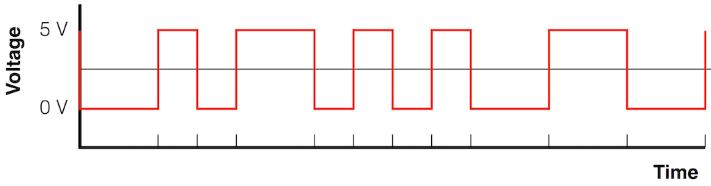
As we saw in the first posting in this series, a theoretical digital transmission system (say, a wire) has an infinite bandwidth, and therefore, if you put a perfect square wave into it, you’ll get a perfect square wave out of it.
Sadly, the difference between theory and practice is that, in theory, there is no difference between their and practice, whereas in practice, there is. In this case, our wire does not have an infinite bandwidth, and so the square wave is not square when it reaches the receiver.
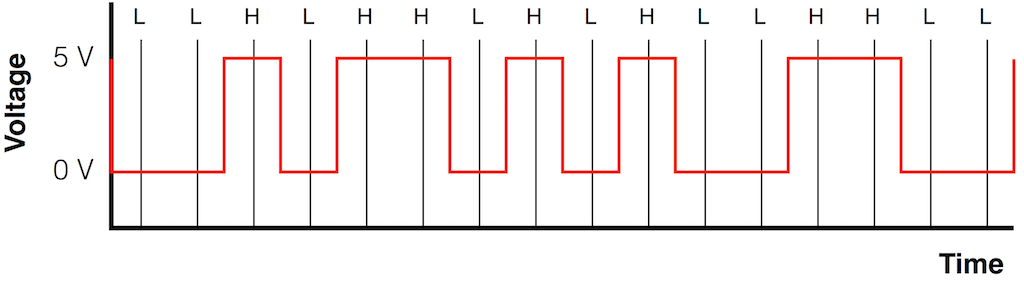
As we saw in the first posting, an S-PDIF signal uses a bi-phase mark, which is the same as saying it’s a frequency-modulated square wave where a “1” is represented by a square wave with double the frequency of a “0”. So, for example, Figure 1 shows one possible representation of the sequence 01011000. (The other possible representation would be the same as this, but upside down, because the first “0” started as a high voltage value.
If that square wave were sent through a wire that rolled off the high frequencies, then the result on the other side might look something like Figure 2.
If we use a detection algorithm that is looking for the moment in time when the incoming signal crosses what we expect to be the half-way point between the high and low voltages, then we get the following
As you can see in Figure 3, the time the transition is detected is late (which is okay) and it varies with respect of the correct time (which is not okay). That variation is the jitter that is caused by the relationship between the pattern in the bi-phase mark, the fundamental frequency of the “square wave” of the carrier (which is related to the sampling rate and the word length, possibly), and the cutoff frequency of the low-pass filter.
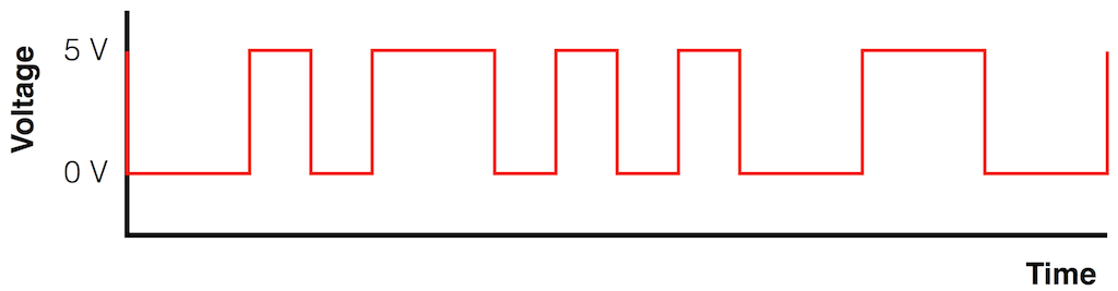
Typically, a digital signal is transmitted using some kind of pulse wave (which is the correct term for what I’ve been calling a “square wave”. It’s a square-ish wave (in that it bangs back and forth between two discrete voltages) but it’s not a square wave because the frequency is not constant. This is true if it’s a non-return-to-zero strategy (where a 1 is represented by a high voltage and a 0 is represented by a low voltage, as shown in Figure 4) or a bi-phase mark (as shown in Figure 1).
In either of these two cases (NRZ or bi-phase mark), the system modulates the amount of time the pulse wave is a high voltage or a low voltage. This modulation is called the duty cycle of the pulse wave. You’ll sometime see a “duty cycle” control on a square wave generator which lets you adjust whether the pulse wave is a square wave (a 50% duty cycle – meaning that it’s high 50% of the time and low 50% of the time) or something else (for example, a 10% duty cycle means that it’s high 10% of the time, and low 90% of the time)
If your transmission system is a little inaccurate, then it could have an error in controlling the duty cycle of the pulse wave. Basically, this means that it makes the transitions at the wrong times for some reason, thus creating a jittered signal before it’s even transmitted.
We’re all familiar with an echo. You stand far enough away from a wall, you clap your hands, and you can hear the reflection of the sound you made, bouncing back from the wall. If the wall is far enough away, then the echo is a second, separate sound from the original. If the wall is close, you still get an echo (in fact, it’s even louder) but it’s coming at you so soon after the original, direct sound, that you can’t perceive it as a separate thing.
What many people don’t know is that, if you stand in a long corridor or a tunnel with an open end, you will also hear an echo, bouncing off the open end of the tunnel. It’s not intuitive that this is true, since it looks like there’s nothing there to bounce off of, but it happens. A sound wave is reflected off of any change in the acoustic properties of the medium it’s travelling through. So, if you’re in a tunnel, it’s “hard” for the sound wave to move (because there aren’t many places to go) and when it gets to the end and meets a big, open space, it “sees” this as a change and bounces back into the tunnel.
Basically, the same thing happens to an electrical signal. It gets sent out of a device, runs down a wire (at nearly the speed of light) and “hits” the input of the receiver. If that input has a different electrical impedance than the output of the transmitter and the wire (on other words, if it’s suddenly harder or easier to push current through it – sort of….) then the electrical signal will (partly) be reflected and will “bounce” back down the wire towards the transmitter.
This will happen again when the signal bounces off the other end of the wire (connected to the transmitter) and that signal will head back down the wire, back towards the receiver again.
How much this happens is dependent on the impedance characteristics of the transmitter’s output, the receiver’s input, and the wire itself. We will not get into this. We will merely say that “it can happen”.
IF it happens, then the signal that is arriving at the receiver is added to the signal that has already reflected off the receiver and the transmitter. (Of course, that combined signal will then be reflected back towards the transmitter, but let’s pretend that doesn’t happen.)
The sum of those two signals is the signal that the receiver tries to decode into a carrier signal. However, the reflected “echo” is a kind of noise that infects the correct signal. This, in turn, can cause timing errors in the detection system of the receiver’s input.
Let’s take a CD player’s S-PDIF output and connect it to the S-PDIF input of a DAC. We’ll use an old RCA cable that we had lying around that has been used in the past – not only as an audio interconnection, but also to tie a tomato plant to a trellis. It’s also been run over a couple of times, under the wheels of an office chair. So, what was once a shield made of nice, tightly braided strands of copper is now full of gaps for electromagnetic waves to bleed in.
We press play on the CD, and the audio signal, riding on the S-PDIF carrier wave is sent through our cable to the DAC. However, the signal that reaches the DAC is not only the S-PDIF carrier wave, it also contains a sine wave that is radiating from a nearby electrical cable that is powering the fridge…
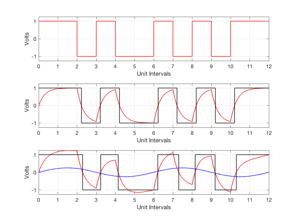
Take a look at Figure 5. The top plot, in red, is the “perfect” carrier wave, sent out by the transmitter.
If that wave is sent through a system that rolls off the high end, the result will look like the red curve in the middle plot. This will be trigger clock events in the receiver, shown as the black curve in the middle plot. There, you may be able to see the intersymbol interference jitter (although it’s small, and difficult to see in that plot).
The blue curve in the bottom plot shows the sinusoidal modulator coming into the system from an external source. That’s added to our low-pass filtered signal, resulting in the red curve in the bottom plot (see how it appears to “ride” the blue curve up and down). The black curve is the end result, triggered by the instances when the red line crosses the mid-point (in this plot, 0 V). You should be able to see there that when the sinusoid is positive, the trigger event is late (relative to what it would have been – the black curve in the middle plot). When the sinusoid is negative, the trigger event is early.
If we take a system that is suffering from
Then the result looks something like Figure 6.
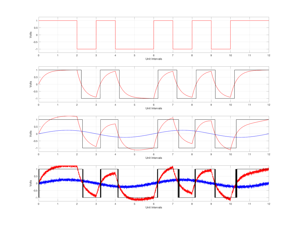
The top plot shows the original bi-phase mark that we intend to transmit.
The second plot shows the low-pass filtered carrier wave (in red) and the triggered events that result (in black).
The third plot shows the periodic, sinusoidal source (in blue), the resulting carrier wave (in red) and the triggered events that result (in black).
The bottom plot adds random noise to the sinusoid (in blue), therefore adding noise to the carrier wave (in red) and resulting in indecision on the transition time. This is because, when the noisy carrier wave crosses the threshold, it goes back and forth across it multiple times per “transition”. So, the black wave is actually banging back and forth between the “high” and “low” values a bunch of times, each time the carrier crosses the threshold. If you are going to build a digital audio receiver that is reasonably robust, you will need to figure out how to deal with this smarter than the way I’ve shown it here.
One of the factors to worry about when you’re thinking about Echo Jitter is the “wavelength” of one “cell”. A cell is the shortest duration of a pulse in the wave (which is half of the duration of a bit – the “high” or the “low” value when transmitting a value of 1 in the bi-phase mark).
This is similar to a real echo in real life. If you clap your hands and hear a distinct echo, then the reflecting surface is very far away. If the echo is not a separate sound – if it appears to occur simultaneously with the direct sound, then the wall is close.
Similarly, if your electrical cable is long enough, then a previous value (a high or a low voltage) may be opposite to the current value sometimes – which may have an effect on the signal at the input of the receiver.
This raises the question: how long is “long”? This can be calculated by finding the wavelength of one cell in the electrical cable when it’s being transmitted.
The speed of an electrical signal in a good conductor is approximately 299,792,458 m/s.
The number of cells per second in an S-PDIF transmission can be calculated as follows:
sampling rate * number of audio channels * 32 bits/frame * 2 cells/bit
This means that the number of cells per second are as follows:
| Fs | Cells per Second |
| 44.1 kHz | 5,644,800 |
| 48 kHz | 6,144,000 |
| 88.2 kHz | 11,289,600 |
| 96 kHz | 12,288,000 |
| 176.4 kHz | 22,579,200 |
| 192 kHz | 24,576,000 |
If we divide the speed of a wave on a wire by the number of cells per second, then we get the length of one cell on the wire, which turns out to be the following:
| Fs | Cell length |
| 44.1 kHz | 53.1 m |
| 48 kHz | 48.8 m |
| 88.2 kHz | 26.6 m |
| 96 kHz | 24.4 m |
| 176.4 kHz | 13.3 m |
| 192 kHz | 12.2 m |
So, even if you’re running S-PDIF at 192 kHz AND if you are getting an echo on the wire (which means that someone hasn’t done a very good job at implementing the correct impedances of the S-PDIF output and input): if your interconnect cable is 30 cm long then you don’t need to worry about this very much (because 30 cm is quite small relative to the 12.2 m cell length on the wire…)
#4 in a series of articles about wander and jitter
Dig out your old cassette copy of “Love Will Keep us Together”, performed by Captain and Tenille (although the original version was released by Neil Sedaka (one of the songwriters) in France) and press PLAY on your oldest cassette deck. You’ll hear the song (now it’s stuck in your head, isn’t it?) as well the hiss from the cassette. That hiss comes (mostly) from the random-ness of the magnetic tape itself, and is just a signal that is added to Captain and Tenille.
Random jitter is similar to the tape hiss. You have a signal (the audio signal that has been encoded as a digital stream of 1’s and 0’s, sent through a device or over a wire as a sequence of alternating voltages) and some random noise is added to it for some reason… (Maybe it’s thermal noise in the resistors, or cosmic radiation left over from the Big Bang bleeding through the shielding of your S-PDIF cable, or something else… )
That random noise results in the device (the audio gear or the chip inside it) wrongly interpreting what time it is, which may or may not affect your audio signal (we’ll talk about that later in the series).
The difference between the cassette example and jitter is that the noise that is modulating the “signal” is not really added to it (at least, it’s not added to the audio signal…). What we’re really talking about is that the jitter is modulating the signal that carries your audio signal – not the audio signal itself. This is an important distinction, so if that last sentence is a little fuzzy, read it again until it makes sense.
Good, I assume that if you’re gotten to this sentence, then you know the difference between the audio signal (the sound of Captain and Tenille singing “Love Will Keep us Together”) and the Carrier signal that is delivering the data that contains that audio signal.
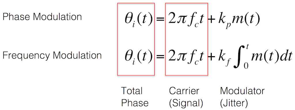
This means that we can talk about the Carrier (for example, the S-PDIF stream of bits that carries the digitally-encoded audio signal) and the Modulator (the signal that changes the timing of that carrier coming in, and thus resulting in jitter).
These are very different – although they look very similar.
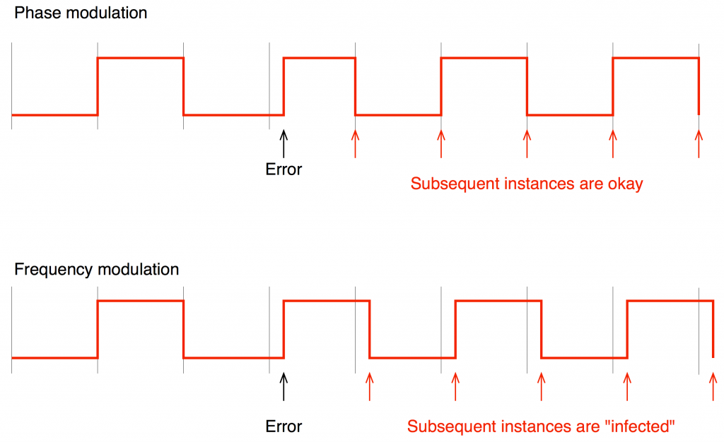
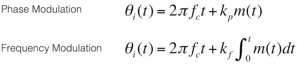
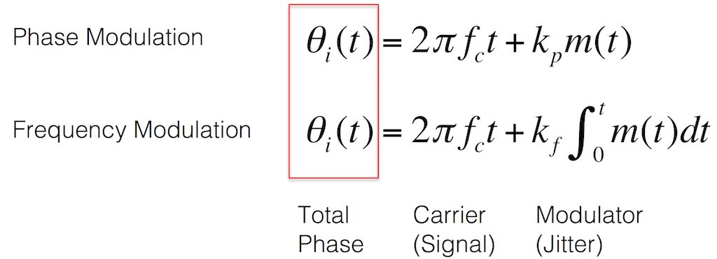
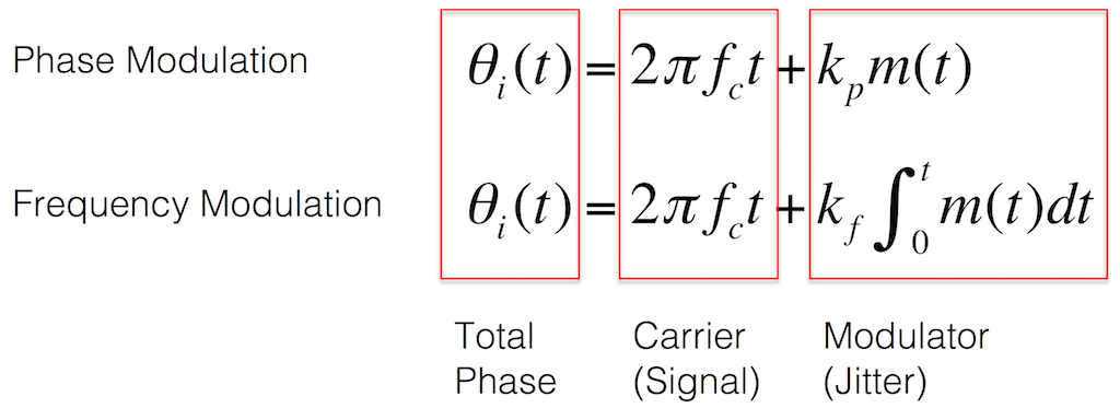
The first is an absolute measure of the error in the clock event – when did that single event happen relative to when it should have happened? Each event can be measured individually relative to perfection – whatever that is. This is called a Phase Modulation of the carrier. It has a Gaussian characteristic (which I’ll explain below…) and has no “memory” (which is explained first).
The second of these isn’t a measure of the events relative to perfection – it’s a measure of the amount of time that happened between consecutive events. This is called a Frequency Modulation of the carrier. It also has a Gaussian characteristic (which I’ll explain below…) but it does have a “memory” (which is explained using Figure 1).
If you stood on a street in New York City and asked the first 100,000 people you saw how much they spent on buying their last car, you would get a very wide range of answers. A very few people who say that they spent a LOT of money. A very few people would say that they spent nothing because they don’t own a car. Most people would give you around the same number, give or take. If we took all of those answers, grouped them into ranges of $100, and plotted the results (therefore showing how many people bought a car that cost $0 – $100, $101 – $200, $201 – $300, and so on… you’d get something like the graph shown in Figure 2.
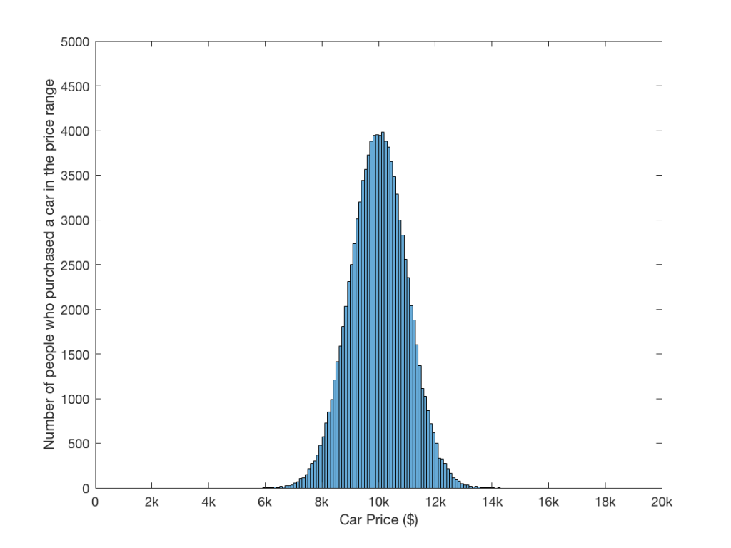
As you can see in the plot in Figure 2, most people spent about $10,000 on their last car. Some some spent more, some spent less… But the further you get from $10,000, the fewer people are “in the club”.
Of course, I made up those numbers – but the important thing is not the actual data – it’s the shape it makes. That “bell curve” is called a “normal distribution” or a “Gaussian distribution” of numbers. If you graph things that occur in nature – everyone’s age in the whole world, the brightness of stars, math grades in Canadian grade 6 students’ final exams, heights of all plants – you’ll see this shape often.
Okay, I lied a little… If you take the ages of everyone in the world, or the heights of all plants, you won’t really get a true Gaussian distribution. This is because, if the values (the ages or the heights) really had a Gaussian distribution, then it would be possible for them to be infinite. Admittedly, the probability of the value being infinite is infinitely small – but that’s a small detail… In addition, the distribution would have to be symmetrical, and since it should be possible to have a value ∞, that would mean that it should also be possible to have a value of -∞ as well…
Let’s get back to Random Jitter… If the jitter is truly random, and we measure the errors in the time events, we will see a Gaussian distribution, centred at 0 seconds. In other words, the error has the highest probability of being 0 (and therefore no error) and the bigger the error (either too early or too late) the smaller the probability of that happening. Weirdly, since the distribution is Gaussian (or at least, we assume that it is) then the worst-case error is -∞ or ∞ – in other words, the event might never happen for some reason – no matter how long you wait…

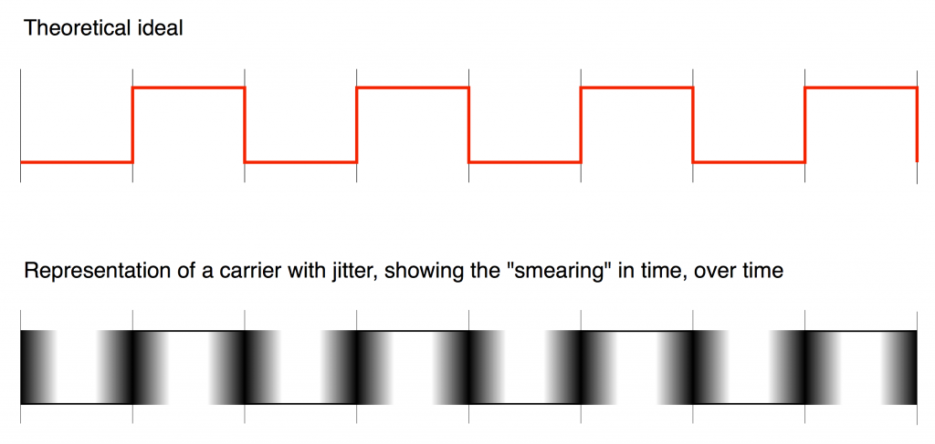
This means that, if you plot a jittered carrier wave on a display, and take a long-exposure photograph of it, you’ll see how the timing events move in time as a “blur” in the photo. A simple artist’s conception (yes, I phrased that correctly…) of this is shown in Figure 4.
This is just a little extra information for geeks and aspiring geeks. If this gives you a headache, ignore it. It will not help you.
#3 in a series of articles about wander and jitter
This posting is a simple one… It’s a setup for the next bunch of postings in this series.
In the last posting, we saw that jitter can be separated into two categories, looking at whether the root of the problem is in the time or the amplitude domain.
A different way to categorise jitter is to start by looking at whether the variation in the timing error is random or deterministic.
If the timing error is random, then there is no way of predicting what the error on the next clock “tick” will be. In this case, the error is caused by some kind of random noise (I know – that’s redundant) somewhere in the system.
However, if it’s deterministic, then the timing error will be correlated with some measurable, interfering signal that is not just random.
One way to think of this is to imagine the sound coming from a poorly-made piece of audio gear.
The signal is what you want to hear.
The other three are things-you-don’t-want-to-hear: stuff that would traditionally be included as TDH+N or “total harmonic distortion plus noise”.
The distortion artefacts are things that are unwanted, but somehow related to the signal – so they are not periodic, but they’re deterministic.
The “hiss” is independent noise – a random signal that is added to (but also unrelated to) your signal.
The hum is not random – it’s periodic (meaning that it repeats itself) – and therefore it’s also deterministic.

If you have a digital audio system, it will have jitter (remember – this might not be anything to worry about… sometimes it just doesn’t matter…). The total jitter that it has is the sum result of all of the different types of jitter that contribute to the total. So, in the chart in Figure 1, you can sort of think of each of the black lines as representing “plus signs”. (Only “sort of”, since it depends on exactly what you’re measuring, and for how long…)
My plan is that I’ll address each of these blocks individually in the coming postings in the series.